 Home
Projects
Publications
Home
Projects
Publications

Start date: Mid-summer 2022
The HP 200A was HP's first product (in 1939), a 35Hz to 35kHz audio oscillator, based on William Hewlett's Masters thesis at Stanford. Plenty more can be read about it on the HP Memory Project, on HP's website, on Ohio University Professor Richard Post's website (which includes pictures of the inside), in William Hewlett's patent, and of course on Wikipedia as well as on many other websites. It was soon followed by the HP 200B, on special order from Walt Disney for the production of Fantasia, with the same specs as the 200A, but a frequency range of 20Hz to 20kHz. More can be read about it on Hewlett Packard Enterprise's website and at the Hewlett-Packard Company Archives Virtual Vault (there is a lot more about the early origins of HP on this website as well). A good video about the origins of HP can be found here, in the first six minutes. The manual for the 200A can be found at the HP Memory Project.
I first heard of positive feedback in my analog electronics course, where it was mentioned it could be used to create oscillators, but was beyond the scope of the course. I recalled having read about the HP 200A while researching HP after buying and fixing my HP 1740A oscilloscope last summer. I began to do more reading about this, learned about Wien-bridge oscillators, Bill Hewlett's lightbulb stabilization (possibly based on Meacham's paper), etc. Producing a sine wave from DC without the use of an inverter seemed very interesting to me, and I also wished to learn more about analog electronics, so I decided to build an oscillator matching the specs of HP's first product, but using modern components, while remaining exclusively analog, and using no ICs other than op-amps.
I began by borrowing Guillermo Gonzales's Foundations of Oscillator Circuit Design from the U of T library, and read through Chapter 1 which discusses relevant control theory and audio oscillator configurations (Wien-bridge, Phase-shift, and Active-filter). I decided on the Wien-Bridge configuration, as it required the fewest changes in component values to change frequencies (only two resistors or two capacitors). I later learned that an oscillating bandpass filter oscillator only requires one resistance value to be changed, but it suffers from other limitations (mainly a limited tuning range). This is discussed in Section 5.3 of "Sinewave Oscillators - Characteristics, Topologies and Examples" by Rod Elliott, which I highly recommend reading. It is the most comprehensive resource I have found regarding audio oscillators.
The Wien-bridge oscillator also happens to be the topology used in the 200A. For reference, the basic circuit is shown here:

Positive feedback occurs at the non-inverting terminal of the op-amp, which provides the phase shift,
and negative feedback at the inverting terminal, which provides the open-loop gain. Applying the Barkhausen criterion shows
that \(A_{vo}=3\) is required for stable oscillations, at a frequency given by \(f_o=\frac{1}{2\pi RC}\).
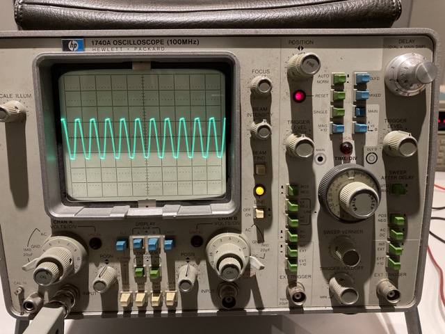
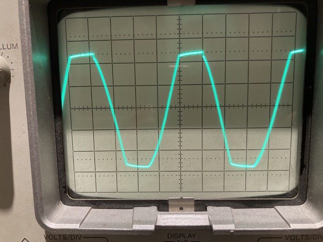
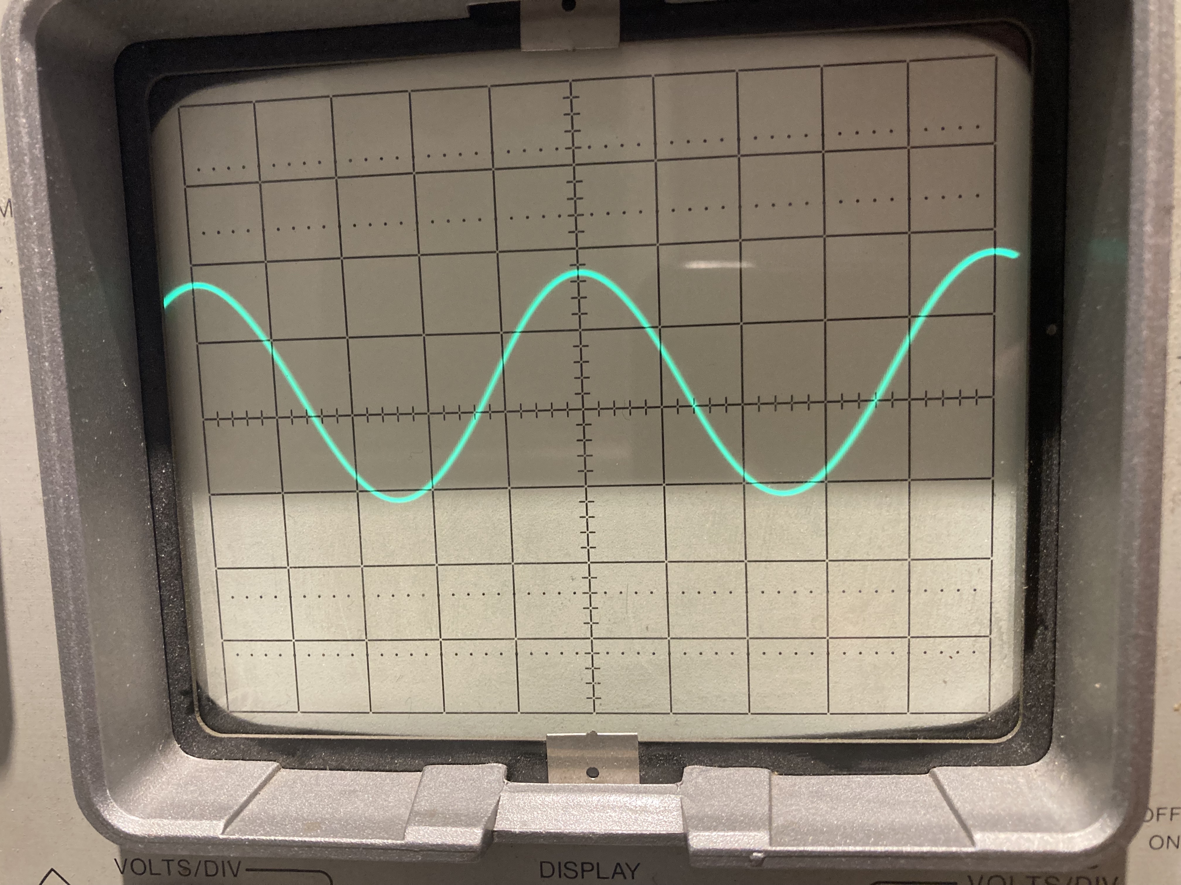
As expected, stable oscillations occur at 10kHz and clipping occurs as the gain is limited solely by the op-amp saturation. To improve this, we need
gain-limiting in the negative-feedback path. A very interesting reference on the subject is Jim Williams's Application Note 43.
I was hesitant to use an incandesent lightbulb as in the original, as they are expensive, increasingly hard to find, and I felt more modern components would be preferable.
I intended to try, but ordered the wrong socket for the 327 bulb, and ordering a new one was prohibitively expensive.
Jim Williams uses a JFET first, then an optocoupler to vary one of the resistances in the negative-feedback
path and he obtains vanishingly low THD.
Contrary to claims I have seen, I was able to obtain <1% with a simple diode solution.
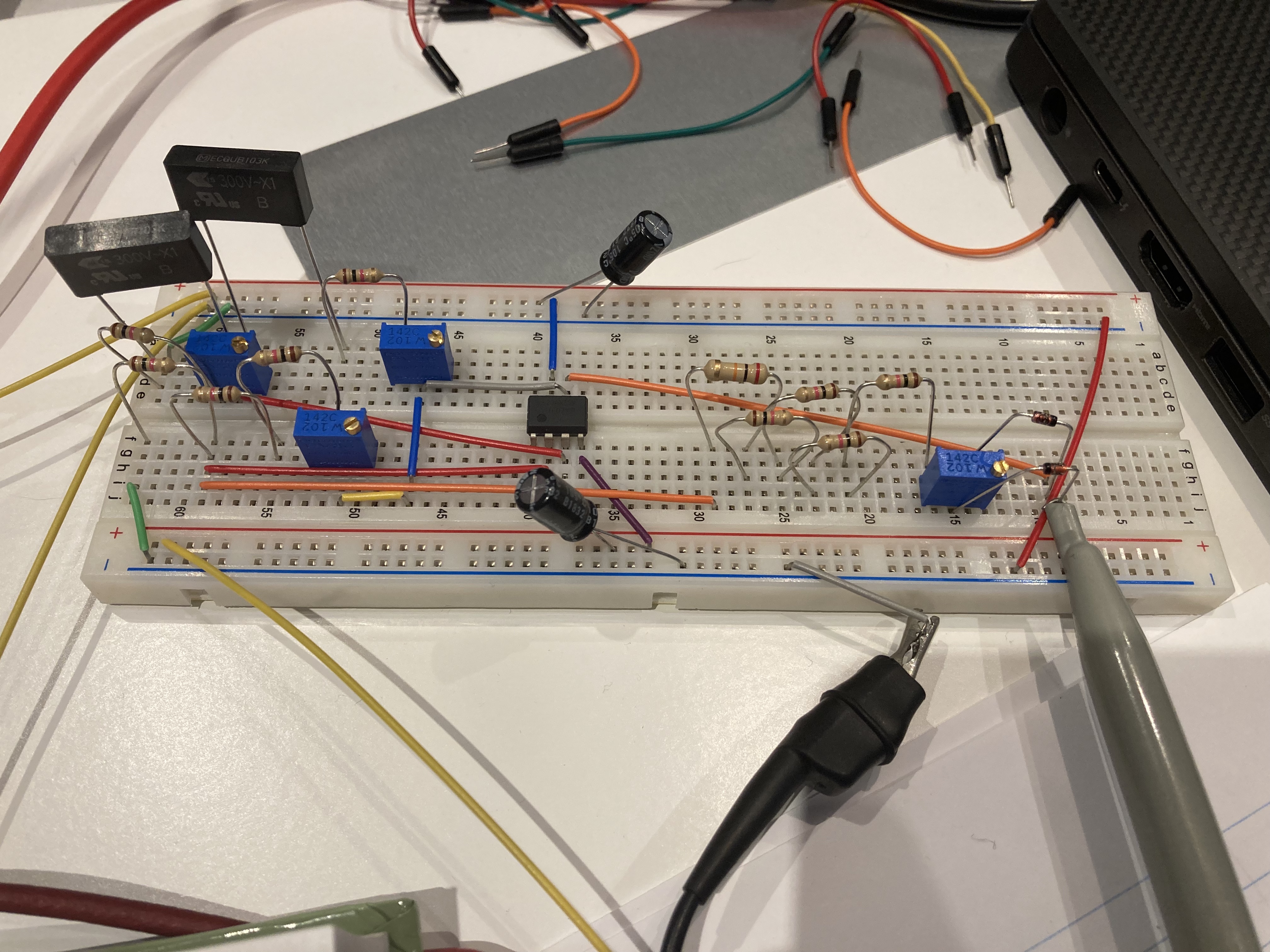
In parallel with \(R_1\), I placed a resistor \(R_3\) in series with two anti-parallel diodes (simple 1N4148s).
This \(R3\) is chosen such that \(\frac{R_2}{R_1||R_3}=1.8\), and all three resistances are then tuned to obtain
optimal distortion characteristics. When the output voltage exceeds a certain amount such that the diodes conduct,
the gain decreases and op-amp clipping is avoided. I tried using 4.3V Zener diodes in series, but THD figures were a little higher,
perhaps different values would improve distortion, but these are expensive to repeatedly purchase.
After some experimentation with various methods, I chose to use the 1N4148s, for simplicity in the implementation, low cost, and availability of parts.
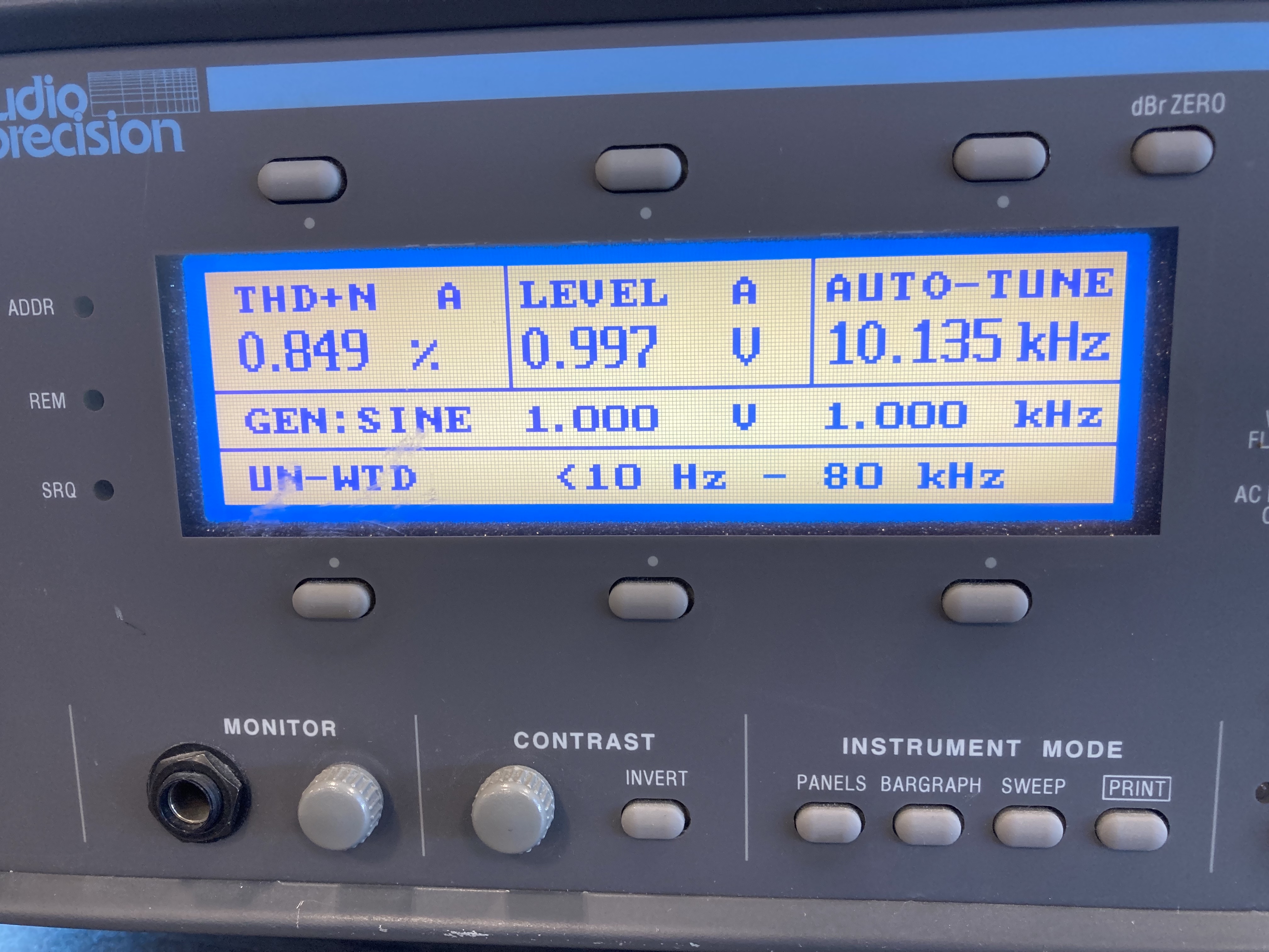
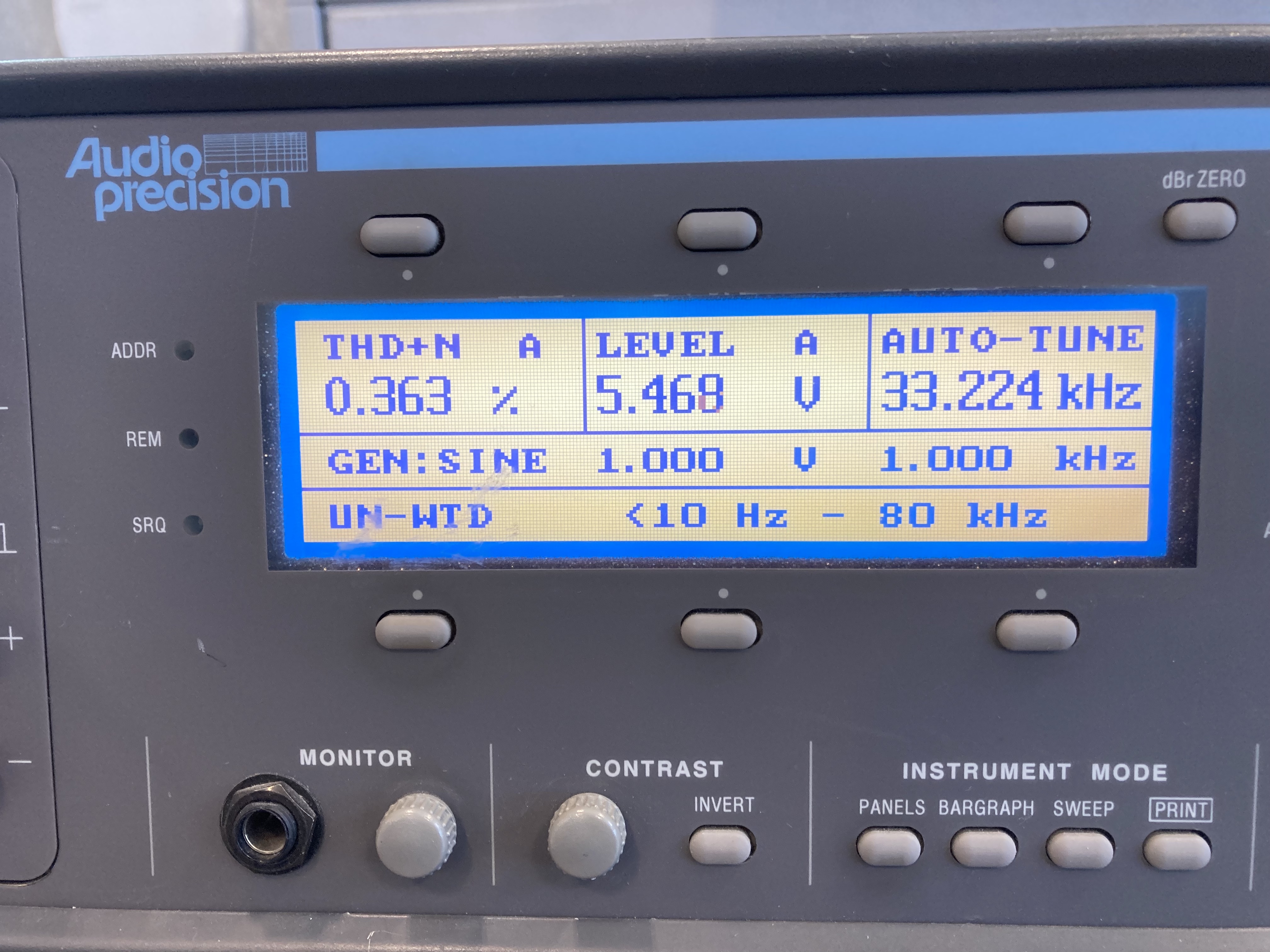
As shown by the Audio Precision ATS-1, a high-end audio analyzer I was able to borrow, THD is <1%, as required.
I initially hoped to use FFT on a DSO, but after trying two different models, I confirmed that they are indeed not precise enough.
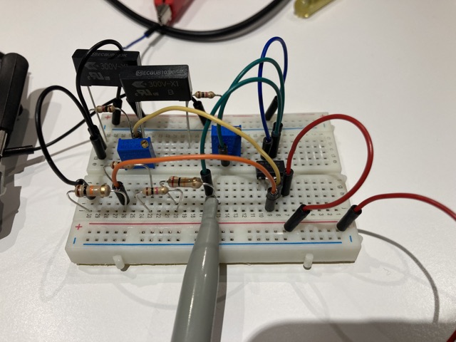
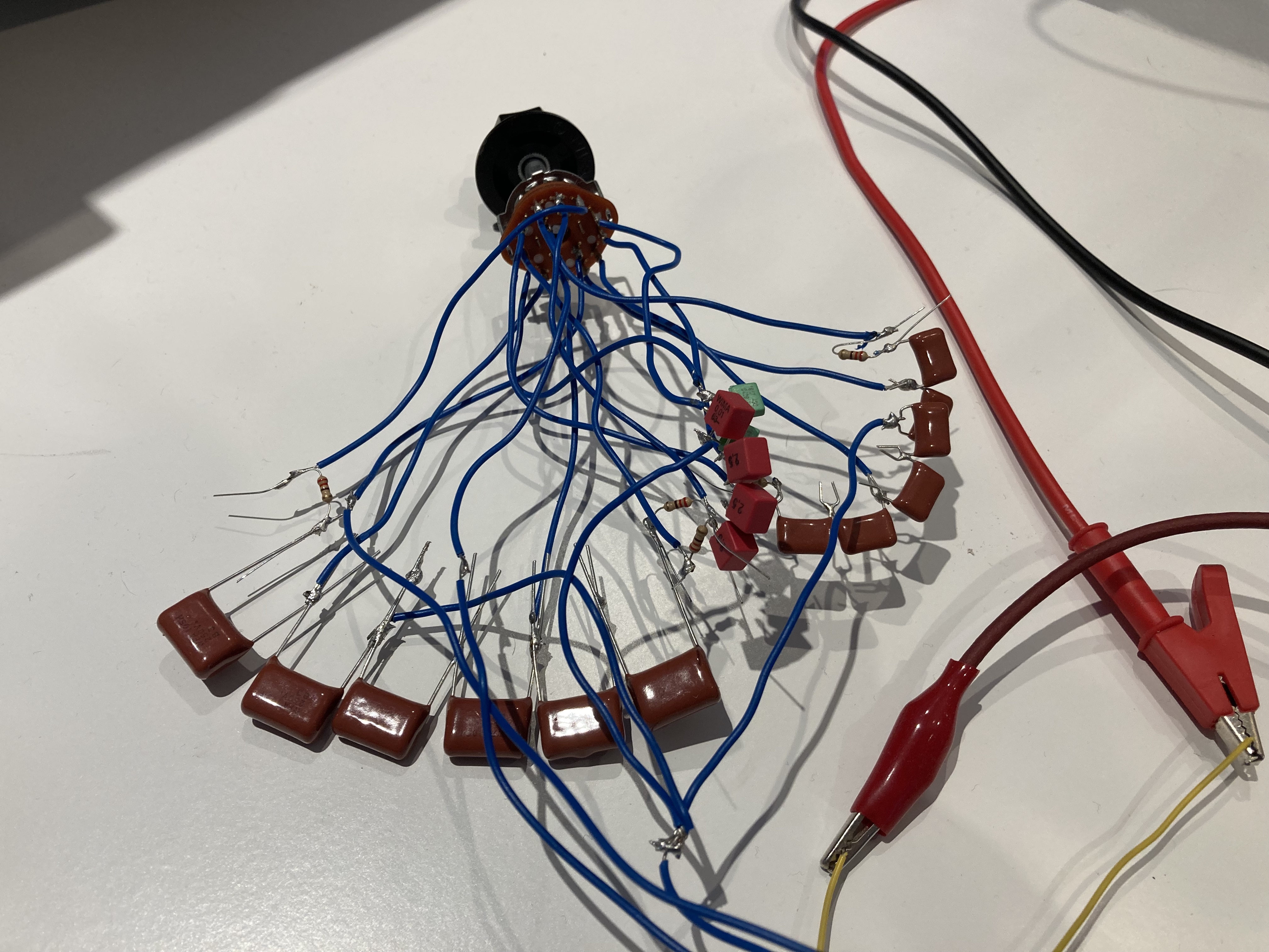
Note also the upgraded breadboard and wires... I was spending more time debugging the cheap breadboard and its wires than the circuit itself.
The addition of a decoupling capacitor on each power rail is also worth noting as they dramatically reduced noise. It is also worth noting that I did not have to
resort to other noise-limiting mechanisms (e.g. bandpass filters).
The next step was stepping up the output to 5Vrms, which was very simple using an op amp on the output.
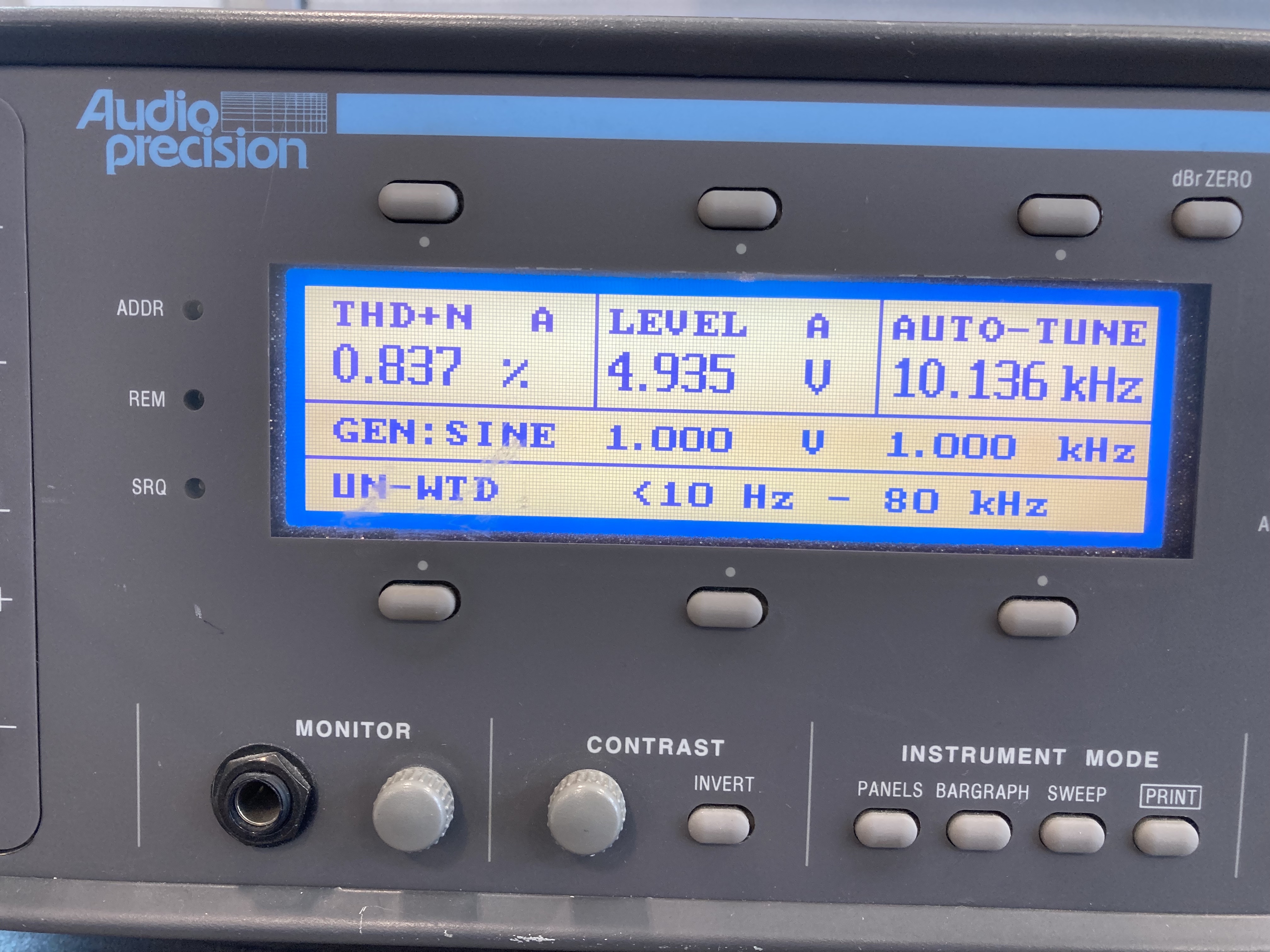
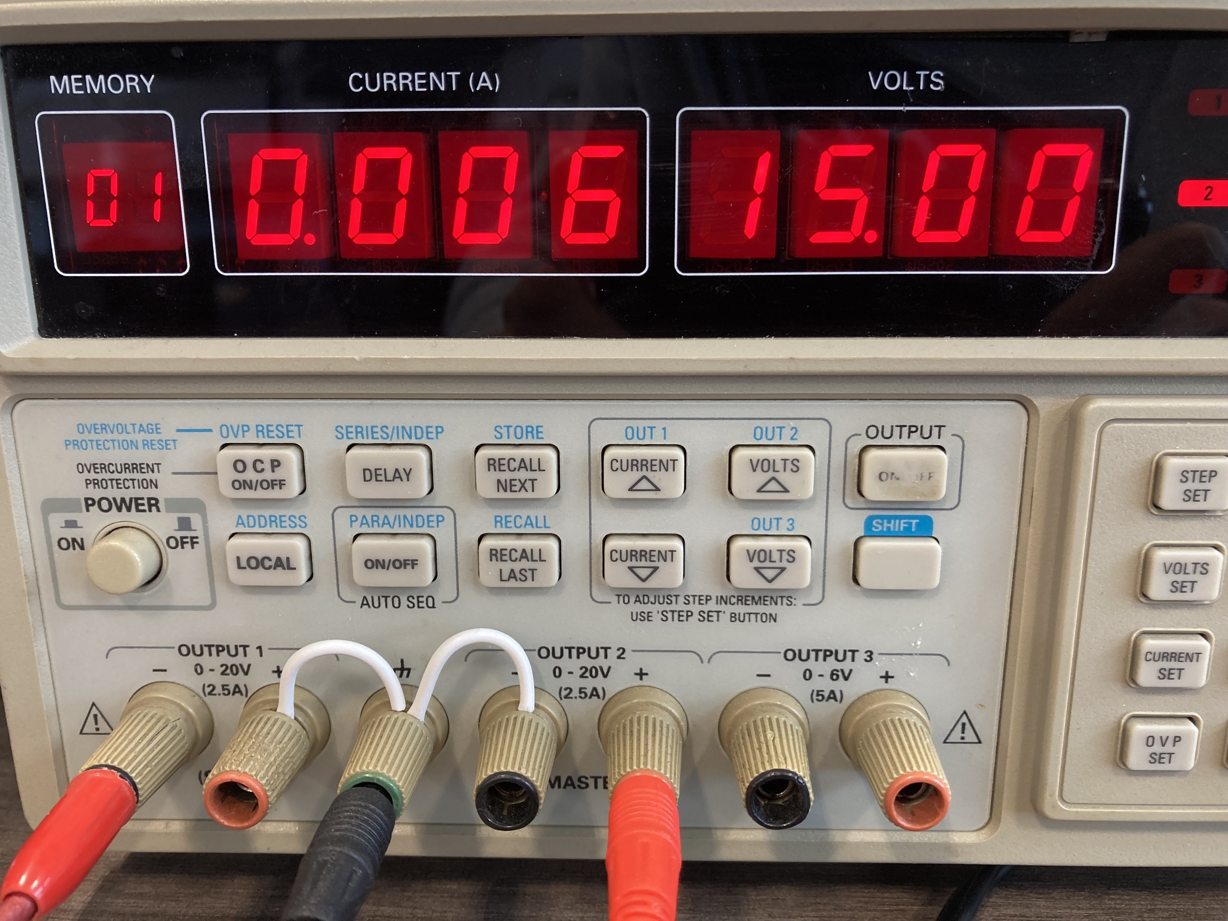
The output op-amp introduces negligible distortion. Current use is also neglgible (6mA), even at 5V, as can be seen on the power supply.
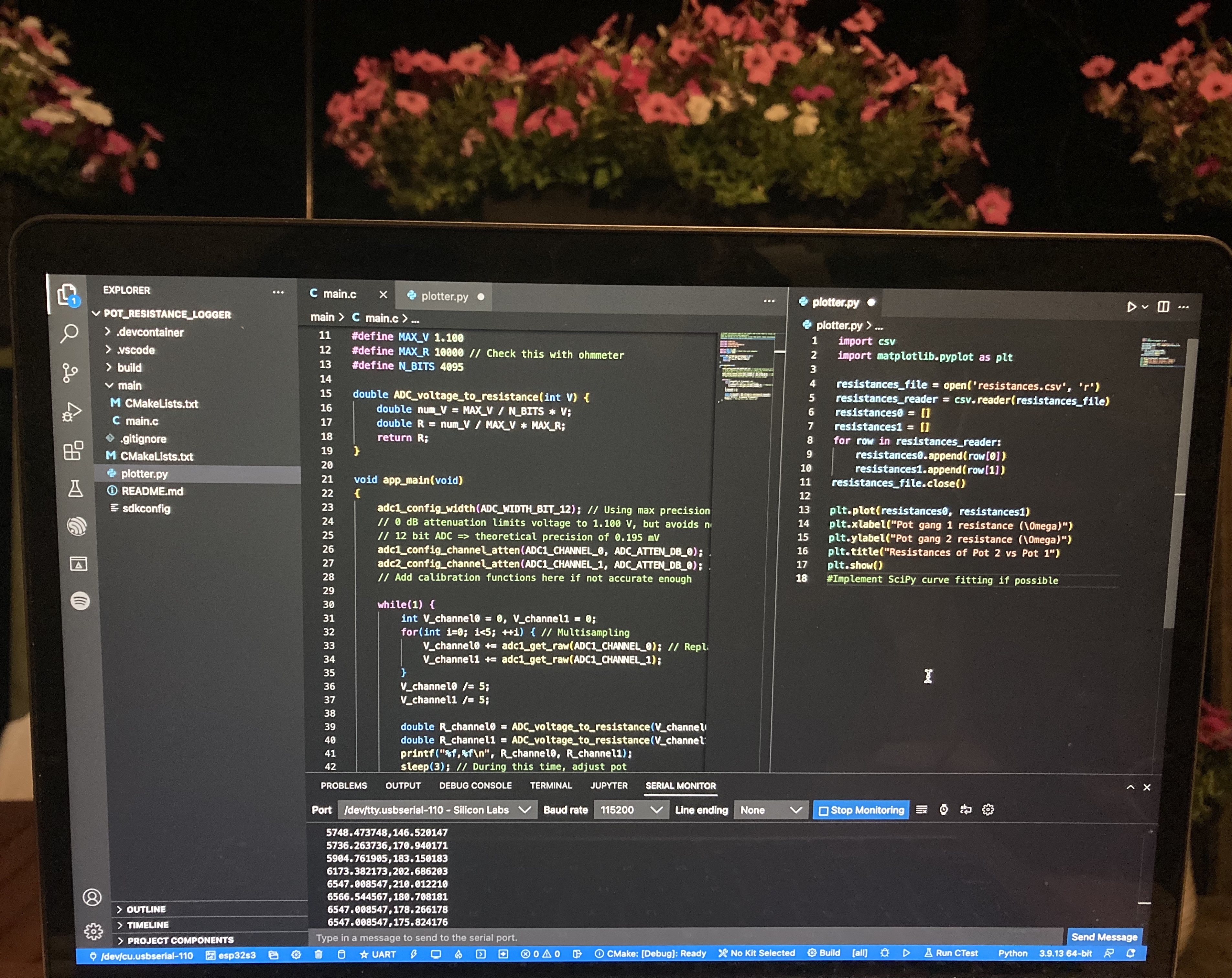
At this point, I purchased different capacitor values to extend the frequency range, and a dual-gang potentiometer to allow for easy frequency adjustment. I also purchased a DP6T rotary switch to select frequency ranges. I had initially bought a DP3T slide switch, but this proved unsuitable as with each change of switch position, the poles become the previous throws, rather than remaining the same poles as I needed. Unfortunately, I soon came to notice a much bigger issue: when turning the potentiometer knob, the output amplitude varies immensely, from over 3V down to 0. This is due to inadequate matching of the two potentiometer gangs. In the 200A, variable capacitors were used, which have much better matching characteristics, but these are difficult to find nowadays and quite large. My potentiometer had the best matching available for a reasonable price (some fancy audio ones cost several hundred $) with a maximum deviation of 3dB. I used an ESP32 to plot the difference between the gang resistances, and noticed variations as large as \(300~\Omega\).
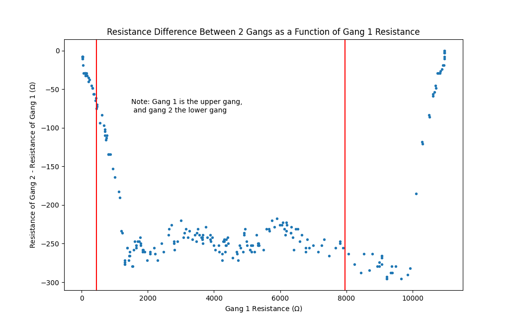
Part of the variation may also be due to the diode gain-limiting, but it is doubtless that the vast majority of it is due to this resistance mismatch. I continued on, and soldered in the switch to allow for switching between each frequency range. I added a \(200\Omega\) resistor in series with most of the capacitors connected to gang 2 to somewhat compensate for the mismatch. I obtained better performance on some of the ranges without this series resistor however, and hence omitted it on those.
This resulted in the following frequency ranges, such that amplitude variation is minimized and stable oscillations are obtained:
| Position | \(C_A=C_B\) (µF) | Frequency range (Hz) |
|---|---|---|
| 1 | 1 | 20 - 185 |
| 2 | 0.5 | 185 - 350 |
| 3 | 0.1 | 200 - 1850 |
| 4 | 0.05 | 1850 - 3500 |
| 5 | 0.01 | 2000 - 18500 |
| 6 | 0.005 | 18500 - 35000 |
I chose to begin by investigating JFETs, which can be used as voltage-controlled resistors (VCRs) over a limited voltage range. They appear to be the 'best' non-IC
option.
Excellent application notes about JFETs can be found here;
the ones by Siliconix are the most useful. One of the application notes also covers the specific VCR use case. JFETs made specifically for VCR applications, such as those
discussed in the Siliconix app note are prohibitively expensive. I instead bought an assortment of various JFETs and set about testing them to see how linear they really were and what resistance range
to expect. I bought those with as high \(r_{DS(on)}\) as possible while remaining affordable.
To test them, I initially hoped to use the DAC on the ESP32 to control the gate-source and drain-source voltage and measure the voltage across a series resistor to calculate current. I could then plot all
this data.
I began writing the code then realized that I have an ESP32-S3... and there is no DAC on that version.
I then hoped to use the GPIB on my power supply, until I realized the cost of USB-compatible GPIB controllers. There are open-source ones on GitHub, and I hope to one day
build one, but for now this remained unfeasible.
I settled for the following circuit:

\(R_{sense}\) is a small resistor on the order of \(6~\Omega\) used for the current measurement. I coded the ESP32 to output a current and voltage measureent every 3 seconds.
During the 3 seconds, I adjust the potentiometer to vary the voltage across the JFET. However, the ESP32's ADC can only measure up to about 950 mV. There are built-in attenuation settings but I
obtained subpar results regardless of the attenuation. I therefore used 2 to 4 \(100~k\Omega\) resistors (large for minimal loading) to make a voltage divider on each pin.
Measuring negative voltages was done using two resistors to average the voltage with a 2V rail.
I saved the current and voltage values in a csv file and used a Python script to plot them.
The first JFET I investigated was an Onsemi J176-D74Z, which is p-channel. Grounding the gate, the JFET is fully on, and results are as follows:
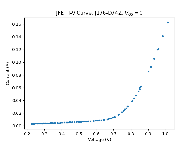
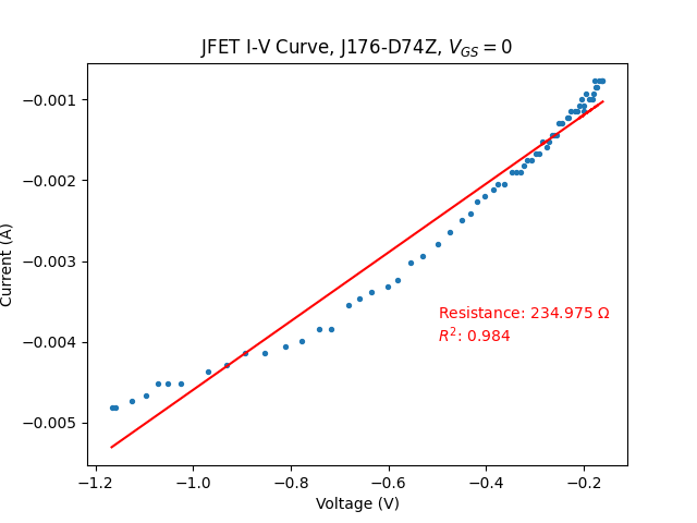
As expected, for positive voltages, the characteristic becomes significantly non-linear around 0.7V, and looks overall exponential. This is because the channel-gate p-n junction becomes forward biased when \(V_{DG}=0.7~V\), and as both drain and source are grounded, \(V_{DG}=V_{DS}\). For negative voltages, the p-n junction is always reverse-biased but the channel becomes increasingly depleted as \(V_{DS}\) decreases, and hence conducts less well. To counter this, we must introduce feedback by adding a large resistor between the source and the gate and an equal resistor between the gate and the drain. An explanation of how this works is provided in the Siliconix VCR app note.
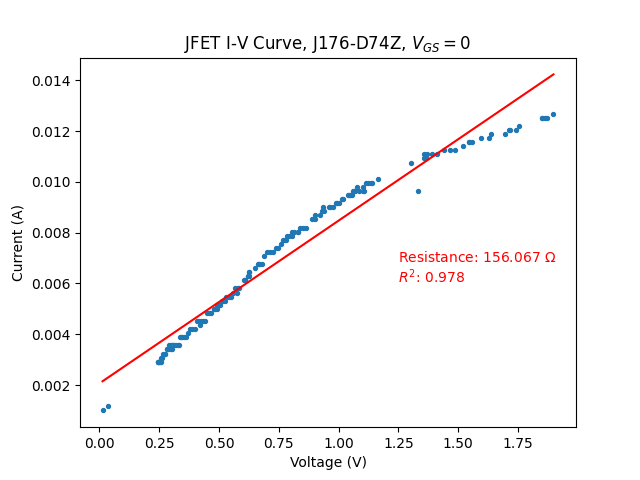
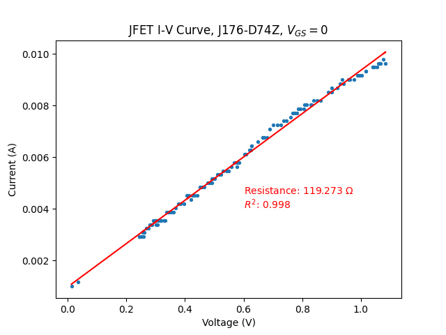
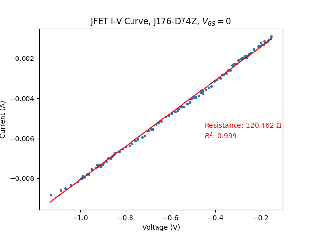
At first glance (leftmost figure), this has improved things somewhat, but the characteristic is still far from linear. However, restricting the voltage range yields excellent linearity, with a very high \(R^2\), and this is true for both positive and negative voltages. Both show about the same resistance, and I attribute the small variation to measurement error as my testing setup is far from ideal. The reason the voltage range must be restricted is that the feedback mechanism can only do so much to counter the deflection, and there comes a point (\(\approx 1~V\)) where it becomes excessively large and it is no longer sufficiently linearized. Note that this means the Wien-Bridge output voltage will have to be attenuated prior to the AGC.
Next, I increased the control voltage (\(V_C\)) using the following circuit:

I obtained the following graphs for negative \(V_{DS}\):
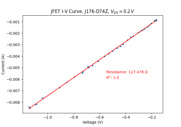
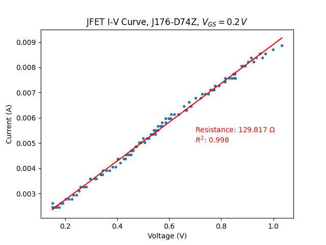
with \(V_{C}=0.2~V\)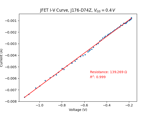
with \(V_{C}=0.4~V\)
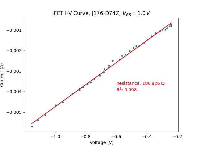
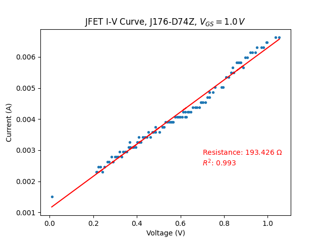
with \(V_{C}=1.0~V\)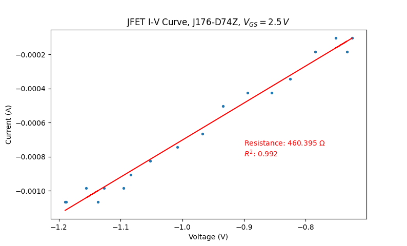
with \(V_{C}=2.5~V\)
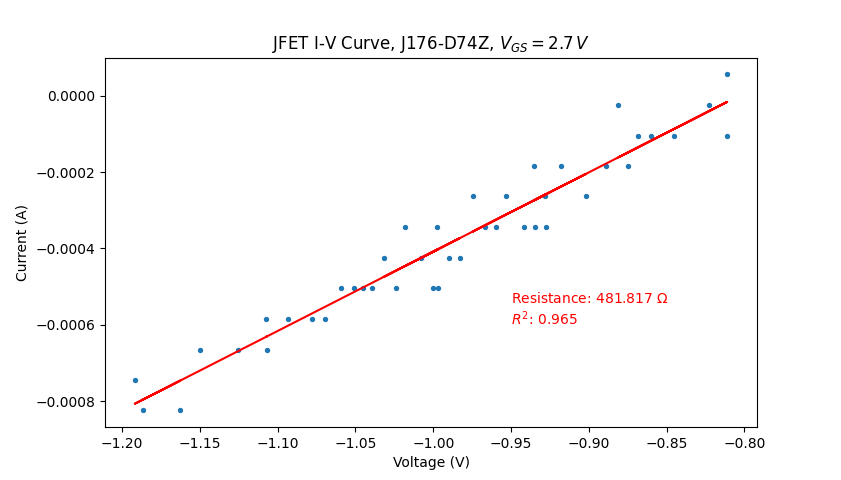
with \(V_{C}=2.7~V\)
Note firstly that I mistakenly labelled the voltage in the titles as \(V_{GS}\) but this should instead be \(V_C\).
Note also that measurement error becomes very significant at \(V_{C}=2.7\,V\). The current appears to move up in steps: this is due to the ADC's resolution limit. Indeed, the voltage increase
across the current-sensing resistor is so small that the ADC does not register it. Note also the very limited voltage range, due to the high resistance of the JFET. These two
effects could be mitigated by adjusting the attenuation circuit and the applied voltage \(V_{DD}\) several times during the measurement. However, the goal is simply to get an idea for the JFET's
I-V curve, not to obtain precise resistance measurements. I therefore continued the same method for positive \(V_{DS}\), and obtained the following graphs:
with \(V_{C}=0.2~V\)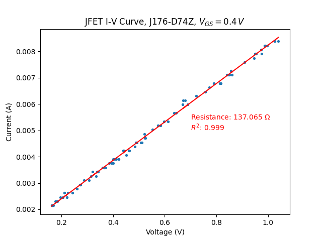
with \(V_{C}=0.4~V\)
with \(V_{C}=1.0~V\)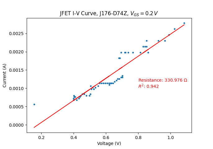
with \(V_{C}=2.5~V\)
Note again the same error: \(V_{GS}\) should be \(V_C\).
Similar limitations are observed at \(V_{C}=2.5V\). The voltage range is somewhat extended as I did change \(V_{DD}\) twice during the test.
Acceptable linearity is present for negative \(V_{DS}\) up to \(V_C=2.7V\), and likely above that although I am limited by my instrumentation. The range appears to be more
limited for positive \(V_{DS}\) but I believe this may be due to instrumentation issues as well, as can be seen on the graph where the current does not change despite increasing \(V_C\).
Plotting the values obtained for negative voltages up to \(V_C=2.5V\) yields:
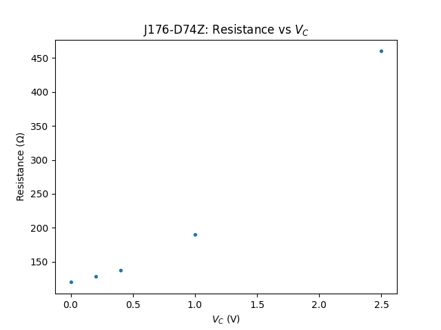
Clearly, \(R_{DS}\) is not a linear function of \(V_{GS}\). This was expected by the formula given in Figure 3 of the Siliconix app note.
It is worth noting that though this particular JFET has these particular characteristics,
other J176-D74Z JFETs may not have identical performance. Indeed, most values are given as ranges in the datasheet.
This component 'matching' is unfortunately quite common in analog audio circuits.
Now that we have a rough idea of the response of this JFET (and pretty graphs), the audio analyzer can be used to characterize distortion performance more accurately (i.e. whether the I-V curve is 'linear enough').
I set up a resistor divider with a grounded JFET-based VCR (i.e. a JFET with the two resistors connected to the gate) connected in series with a \(500~\Omega\) resistor. I applied a low-distortion 1V sine wave
produced by the audio analyzer (THD=0.0025% at 1V and 1kHz) and obtained the following results:
| JFET Resistance (\(\Omega\)) | |||
|---|---|---|---|
| 20Hz | 1kHz | 35kHz | |
| 131 | 0.024 | 0.104 | 0.115 |
| 144 | 0.030 | 0.159 | 0.113 |
| 158 | 0.044 | 0.215 | 0.110 |
| 226 | 0.237 | 0.473 | 0.0975 |
| 1202 | 6.82 | 6.85 | 2.50 |
The trend is as expected: as resistance goes up, so does distortion. However, THD in the kHz is higher than I had hoped, especially at resistances that remain rather low (\(\approx 200~\Omega\)).
I worry that the THD introduced by the oscillator, a gain stage to reduce the signal to under 1V, at least one AGC stage, and a second gain stage to amplify it to a 5V output will introduce excessive THD.
If I must restrict my resistance range to something along the lines of \(120~\Omega < R < 200~\Omega\), I worry about the number of AGC stages that may be required (and the large associated distortion and cost).
I likely need to further reduce my applied voltage, indeed it is often recommended to limit operation to under 100mV, or even 10mV for JFET-based VCRs. I also suspect shunting the control voltage with a decoupling capacitor may improve things somewhat. Perhaps adding a smal
potentiometer to adjust the feedback resistance empirically may also help.
I should also add a capacitor in series between the input signal and the signal-to-gate feedback resistor to limit control voltage feedthrough, but this shouldn't affect THD.
Unfortunately, I no longer have access to the audio analyzer. Once I find an affordable one, I will return to this project.